Details
-
Spike
-
 Should have
-
None
-
Obs Mgt & Controls
-
-
-
2
-
2
-
3
-
1.5
-
Team_CIPA
-
Sprint 5
-
-
-
The TDC bitstream was integrated with support for VCC processing from one 100GbE dish input, and FSP processing for up to 8 antenna.
Modules integrated include
- VCC Channelizer for one receptor
- Frequency slice circuit switch for 10 coarse channels
- ReSampler/Delay Tracker for 8 receptors,
- 16K Fine Channelizer for 8 receptors,
- Fine Channel Corner Turn for 8 receptors,
- TDC Correlator for 8 receptors, 14480 fine channels.
- Visibility Transport over SLIM optical interface.
- SPEAD Packetisation for Visibilities according to ICD.
With the increase in FPGA resource utilisation the Quartus tool has to work harder to meet timing for the digital logic to work correctly at the required operational clock frequency. To make meeting timing easier (or possible) changes to the logic are required over many iterations. Significant changes to improve timing were made to:
- Resampler/Delay Tracker - improved control signal generation to reduce critical path lengths.
- Circuit Switch - new crossbar architecture to reduce routing congestion.
- 16k Fine Channelsier - reset minimisation to reduce reset net fanout.
Many additional pipeline stages were added to many modules to allow quartus more freedom to place the logic around the chip.
Resource usage of the FPGA has reached approximately 50%, and with changes to the logic the timing is very close to being met, and with additional effort requested from Quartus (additional hour compile time - 5hr40m total) then timing closure is often achieved.
Logic utilization (in ALMs) 473,188 / 933,120 ( 51 % )
Logic utilization (in ALMs) 473,188 / 933,120 ( 51 % )
Total dedicated logic registers 1386736
Total pins 949 / 1,152 ( 82 % )
Total block memory bits 146,700,816 / 240,046,080 ( 61 % )
Total RAM Blocks 8,505 / 11,721 ( 73 % )
Total DSP Blocks 1,627 / 5,760 ( 28 % )
Total HSSI RX channels 16 / 96 ( 17 % )
Total HSSI TX channels 16 / 96 ( 17 % )Routing Utilisation looks reasonably good. Some areas of heavy utilisation, particularly around the DDR4 interfaces.
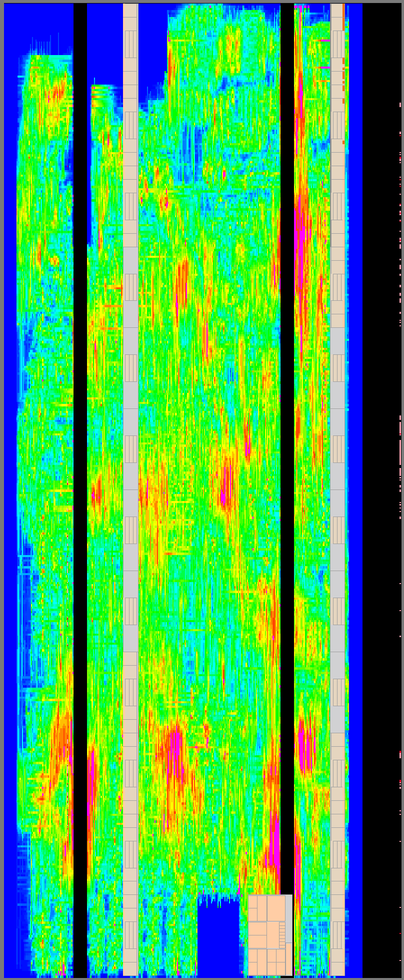 The TDC bitstream was integrated with support for VCC processing from one 100GbE dish input, and FSP processing for up to 8 antenna. Modules integrated include VCC Channelizer for one receptor Frequency slice circuit switch for 10 coarse channels ReSampler/Delay Tracker for 8 receptors, 16K Fine Channelizer for 8 receptors, Fine Channel Corner Turn for 8 receptors, TDC Correlator for 8 receptors, 14480 fine channels. Visibility Transport over SLIM optical interface. SPEAD Packetisation for Visibilities according to ICD. With the increase in FPGA resource utilisation the Quartus tool has to work harder to meet timing for the digital logic to work correctly at the required operational clock frequency. To make meeting timing easier (or possible) changes to the logic are required over many iterations. Significant changes to improve timing were made to: Resampler/Delay Tracker - improved control signal generation to reduce critical path lengths. Circuit Switch - new crossbar architecture to reduce routing congestion. 16k Fine Channelsier - reset minimisation to reduce reset net fanout. Many additional pipeline stages were added to many modules to allow quartus more freedom to place the logic around the chip. Resource usage of the FPGA has reached approximately 50%, and with changes to the logic the timing is very close to being met, and with additional effort requested from Quartus (additional hour compile time - 5hr40m total) then timing closure is often achieved. Logic utilization (in ALMs) 473,188 / 933,120 ( 51 % ) Logic utilization (in ALMs) 473,188 / 933,120 ( 51 % ) Total dedicated logic registers 1386736 Total pins 949 / 1,152 ( 82 % ) Total block memory bits 146,700,816 / 240,046,080 ( 61 % ) Total RAM Blocks 8,505 / 11,721 ( 73 % ) Total DSP Blocks 1,627 / 5,760 ( 28 % ) Total HSSI RX channels 16 / 96 ( 17 % ) Total HSSI TX channels 16 / 96 ( 17 % ) Routing Utilisation looks reasonably good. Some areas of heavy utilisation, particularly around the DDR4 interfaces.
 -
13.6
-
Stories Completed, Integrated, Outcomes Reviewed, Satisfies Acceptance Criteria, Accepted by FO
Description
This spike is a background activity for PI13 to continue to progress the work done in PI13 on the TDC AA0.5/AA1 correlation bitstream. This spike requires small amounts of periodic work with lengthy FPGA compiles in between. The primary objective is to identify timing issues, and address them if time permits within the committed work for PI13.
- Integrate FW IP blocks into TDC AA0.5/AA1 correlation bitstream as they become available.
- Perform bitstream compilation to determine monitor resource usage and timing closure
- Generate plans to address timing issues
- Address timing issues if time permits in PI13
- Repeat
